Produktbeskrivning
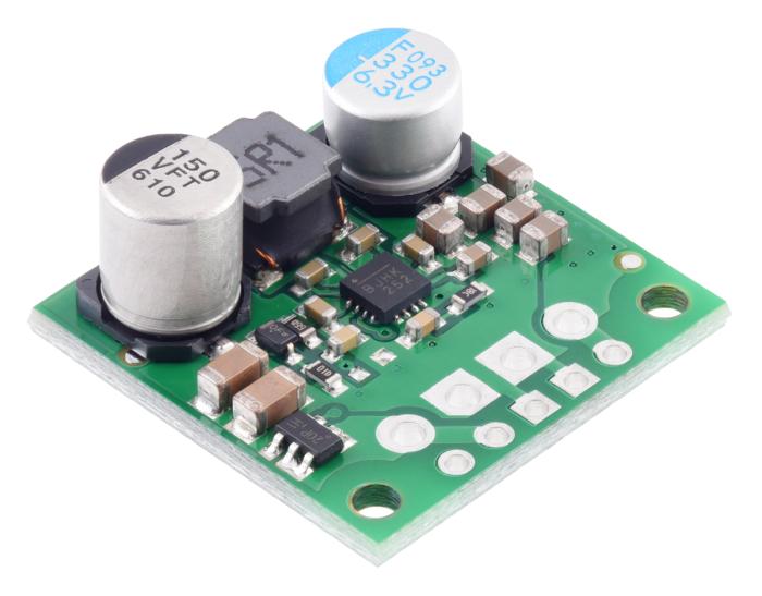
This powerful synchronous switching step-up/step-down regulator efficiently produces 5 V from input voltages between 2.8 V and 22 V. Its ability to convert both higher and lower input voltages makes it useful for applications where the power supply voltage can vary greatly, as with batteries that start above but discharge below 5 V. The board measures 0.9" × 0.9", has a typical efficiency of 85% to 95%, and can supply typical continuous output currents between 2 A and 4 A depending on the input voltage. The regulator also features reverse voltage protection and an optional enable input that can be used to put the regulator in a low-power state with a current draw of less than 10 µA per volt on VIN.
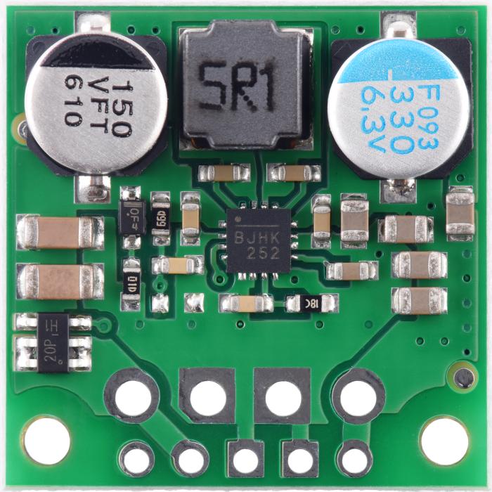
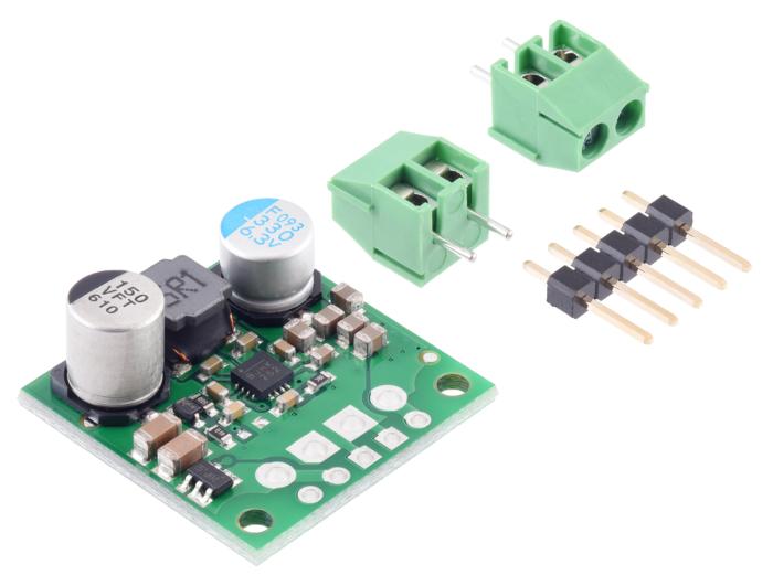
The step-up/step-down regulator has four connections: enable (EN), the input voltage (VIN), ground (GND), and the output voltage (VOUT). The input voltage, VIN, powers the regulator. Voltages between 2.8 V and 22 V can be applied to VIN. VOUT is the regulated output voltage.
The regulator, which is enabled by default, can be put into a low-power sleep state by bringing the EN pin low. The rising threshold for the EN pin is between 1 V and 1.2 V, and the falling threshold is at most 160 mV lower than that (i.e. the falling hysteresis is 160 mV max). This allows a precise low-VIN cutoff to be set, such as with the output of an external voltage divider powered by VIN, which can be useful for battery powered applications where draining the battery below a particular voltage threshold could permanently damage it. The quiescent current draw in sleep mode is dominated by the current in the 475 kO pull-up resistor from ENABLE to VIN and in the reverse-voltage protection circuit, which altogether will be between 2 µA and 10 µA per volt on VIN.
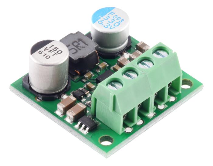
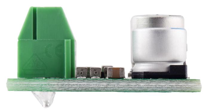
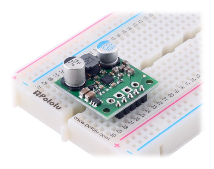
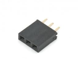
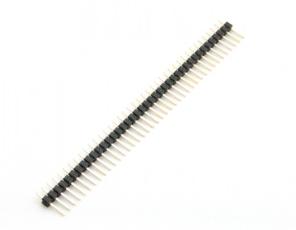
The regulator has two sets of through-holes: five smaller holes arranged with a 0.1" spacing along the edge of the board (for compatibility with standard solderless breadboards and perfboards and connectors that use a 0.1" grid) and four larger holes intended for 3.5 mm-pitch terminal blocks. VIN, GND, and VOUT are available at both the smaller holes and larger holes, but EN is only available on the smaller row of through-holes.
* Input voltage: 2.8 V to 22 V
* Output voltage: 5 V with 3% accuracy
* Typical maximum continuous output current: 2 A to 4 A, depending on input voltage
* Typical efficiency of 85% to 95%, depending on input voltage and load
* 10 mA to 20 mA typical no-load quiescent current; can be reduced to 2 µA to 10 µA per volt on VIN by disabling the board
* Input under-voltage lockout and output over-voltage protection
* Soft-start feature limits inrush current and gradually ramps output voltage
* Integrated reverse-voltage protection up to 20 V, over-current protection, and over-temperature shutoff
* Fixed switching frequency of ~500 kHz
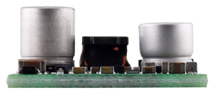
* Compact size: 22.9 mm × 22.9 mm × 9.7 mm
* Two 0.086" mounting holes for #2 or M2 screws

